


Summary
- Sony Semiconductor Solutions application published on 22 December 2022
- Tapered metal walls reflect oblique light toward the photodiode
- The goal is to reduce losses and limit optical crosstalk
- The technical example uses a 120 × 300 nm wall and an angle of about 52 degrees
- No commercial sensor or product has been announced
A Sony Semiconductor Solutions patent application describes tapered walls between pixels that reflect oblique light toward the photodiode and limit losses as sensors become denser.
What the patent describes
Application US20220406832A1, titled “Image sensor and imaging device,” was published in the United States on 22 December 2022. Hiroshi Tanaka, Yusuke Moriya and Takushi Shigetoshi are listed as inventors, with Sony Semiconductor Solutions as the assignee. It was filed on 15 September 2020, claims priority from 21 November 2019 and remains pending.
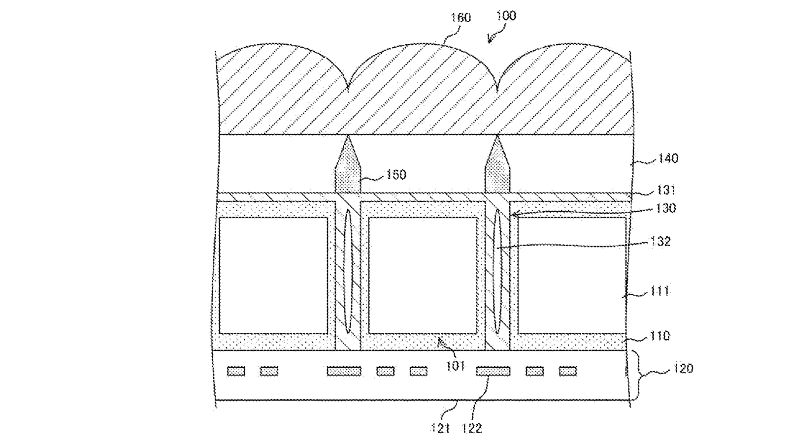
The central idea is a metal isolation wall at each pixel boundary. Instead of vertical sidewalls, the element is tapered so that the upper opening toward the microlens differs from the lower opening toward the photodiode.
How the tapered walls work
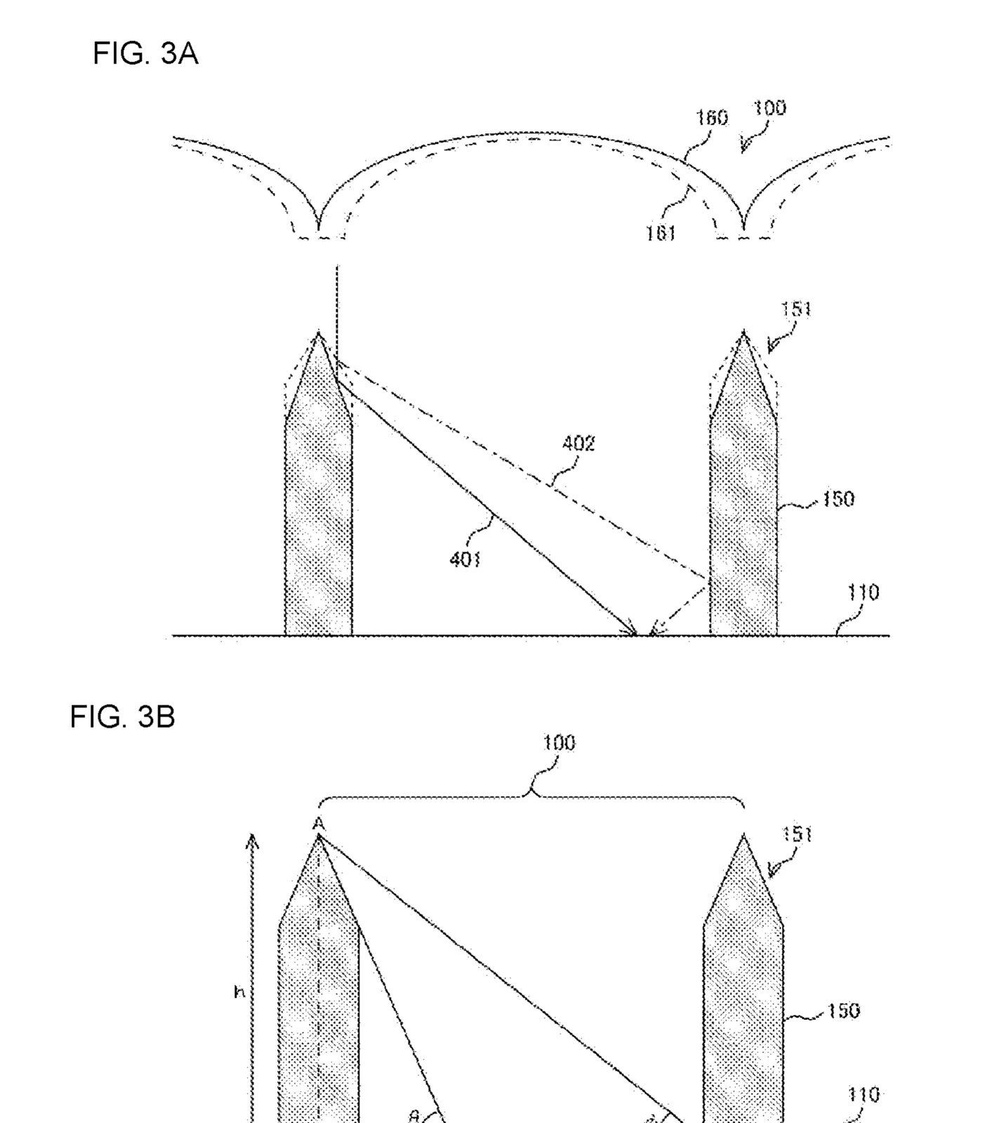
The microlens directs incoming light toward the photosensitive area. A ray arriving at a steep angle may strike the pixel boundary rather than the photodiode. The patent’s inclined reflective surface turns that ray inward, generally aiming to require only one reflection.
In one numerical example, the wall is 120 nm wide and 300 nm high, the pixel’s light-receiving surface is 1,500 nm wide and the insulating layer is 100 nm thick. The resulting elevation angle is approximately 52 degrees.
Why small pixels lose photons
As pixels shrink, their active opening becomes smaller and oblique light is harder to guide into the correct photodiode. Conventional metal structures may absorb part of the energy, especially when a ray reflects several times before reaching its target.
Sony’s geometry attempts to reduce the number of reflections. The expected benefit is more usable light energy in the correct pixel while preserving separation from its neighbour.
What it means for crosstalk and sensitivity
Optical crosstalk occurs when light intended for one pixel reaches a neighbouring pixel. This can affect colour accuracy and light-collection efficiency. The proposed wall acts both as a barrier and a reflector, stopping leakage while redirecting part of the light into the correct photodiode.
The application provides no commercial measurements in stops, dynamic range or noise. Its description therefore cannot be translated into a specific camera-performance gain.
Where it could be used
The technique is described in relation to a backside-illuminated sensor and could theoretically suit systems where pixel density and oblique-angle efficiency matter. That includes small sensors in portable devices as well as other imaging applications.
The patent names no smartphone, camera or commercial sensor. It also confirms no production timetable or partnership with a device maker.
A patent is not a product
Publishing an application shows that a company protected a technical approach, not that it decided to use it. Many patents remain defensive, evolve in another form or never reach a product.
This is not a new 2026 announcement. The filing claims 2019 priority and was published in 2022 before resurfacing in the news. That distinction matters because the technology is not an immediate preview of a new sensor.
What we think
The intriguing part is how the patent addresses an optical problem through geometry at a scale of hundreds of nanometres. Rather than relying only on improved materials or more computational processing, it aims to manage the path of light inside each pixel more efficiently.
Its practical value will only become clear with real measurements and a commercial sensor. Until then, it is a technical window into Sony’s research rather than a promise for the next camera or smartphone.
Frequently asked questions
What is application US20220406832A1?
It is a Sony Semiconductor Solutions patent application for an image sensor and imaging device using tapered isolation walls between pixels.
How do the tapered walls help?
They reflect oblique light toward the photodiode while limiting leakage into neighbouring pixels.
Is there already a product using this technology?
The application identifies no commercial sensor, camera or smartphone and confirms no production schedule.
Is this a new 2026 patent?
No. Its priority dates to 2019, it was filed in 2020 and published in the United States in 2022.